| CPC H01L 33/387 (2013.01) [H01L 27/156 (2013.01); H01L 33/005 (2013.01); H01L 33/405 (2013.01); H01L 33/62 (2013.01); H01L 2933/0016 (2013.01)] | 20 Claims |
|
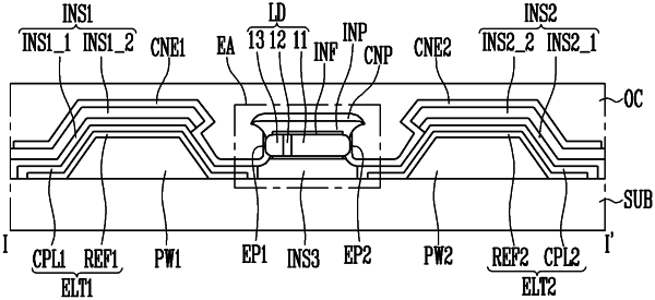
1. A light emitting device comprising:
a first electrode and a second electrode disposed on a substrate and spaced apart from each other;
at least one light emitting diode disposed between the first electrode and the second electrode, the at least one light emitting diode including a first end and a second end on sides in a longitudinal direction of the at least one light emitting diode;
an insulating pattern overlapping an upper portion of the at least one light emitting diode and exposing the first and the second ends of the at least one light emitting diode;
a first contact electrode electrically connecting the first end of the at least one light emitting diode to the first electrode; and
a second contact electrode electrically connecting the second end of the at least one light emitting diode to the second electrode, wherein
the insulating pattern completely overlaps the first and the second ends of the at least one light emitting diode in a plan view, and
the insulating pattern has a shape in which a width of the insulating pattern reduces toward a lower portion of the insulating pattern in a cross-sectional view.
|