| CPC H01L 33/382 (2013.01) [H01L 25/0756 (2013.01); H01L 27/156 (2013.01); H01L 33/06 (2013.01); H01L 33/08 (2013.01); H01L 33/14 (2013.01); H01L 33/387 (2013.01)] | 19 Claims |
|
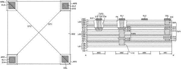
1. A light emitting device comprising:
a first light emitting part including a first conductivity-type semiconductor layer, a first active layer, a second conductivity-type semiconductor layer, and a first ohmic electrode;
a second light emitting part disposed over the first light emitting part and including a first conductivity-type semiconductor layer, a second active layer, a second conductivity-type semiconductor layer, and a second ohmic electrode;
a third light emitting part disposed over the second light emitting part and including a first conductivity-type semiconductor layer, a third active layer, a second conductivity-type semiconductor layer, and a third ohmic electrode;
a common electrode pad electrically connected to the second conductivity-type semiconductor layer of each of the first, second, and third light emitting parts;
a first electrode pad electrically connected to the first conductivity-type semiconductor layer of the first light emitting part;
a second electrode pad electrically connected to the first conductivity-type semiconductor layer of the second light emitting part; and
a third electrode pad electrically connected to the first conductivity-type semiconductor layer of the third light emitting part,
wherein the light emitting device has substantially a quadrangular shape when viewed from the top, and has first, second, third, and fourth corners, and
wherein a length between first and second corners of the third light emitting part is less than a length between the third and fourth corners of the light emitting device.
|