| CPC H01L 33/38 (2013.01) [H01L 33/00 (2013.01); H01L 33/24 (2013.01); H01L 33/62 (2013.01)] | 5 Claims |
|
1. An ultraviolet (UV) light emitting diode comprising:
a substrate;
an n-type semiconductor layer disposed on the substrate;
a mesa disposed on the n-type semiconductor layer and comprising an active layer and a p-type semiconductor layer;
an n-ohmic contact layer contacting the n-type semiconductor layer;
a p-ohmic contact layer contacting the p-type semiconductor layer;
an n-bump electrically connected to the n-ohmic contact layer; and
a p-bump electrically connected to the p-ohmic contact layer,
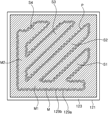
wherein the mesa comprises a plurality of branches,
the n-ohmic contact layer surrounds the mesa and is disposed in a region between the branches,
each of the n-bump and the p-bump covers an upper surface and a side surface of the mesa, and
the p-bump covering at least two of the branches among the plurality of branches.
|