| CPC H01L 33/10 (2013.01) [H01L 33/405 (2013.01); H01L 33/48 (2013.01); H01L 33/38 (2013.01)] | 18 Claims |
|
1. A semiconductor device, comprising:
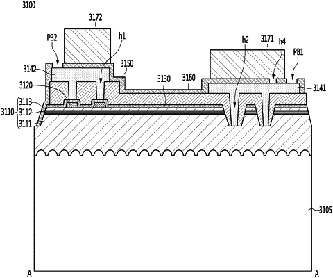
a light emitting structure comprising a first conductivity type semiconductor layer, an active layer disposed on the first conductivity type semiconductor layer, and a second conductivity type semiconductor layer disposed on the active layer, wherein the light emitting structure further comprises a plurality of recesses passing through the second conductivity type semiconductor layer and the active layer to expose a portion of the first conductivity type semiconductor layer;
a light transmitting electrode layer disposed on the light emitting structure;
a reflective layer disposed on the light transmitting electrode layer, and comprising a plurality of first openings exposing an upper surface of the light transmitting electrode layer and a plurality of second openings exposing an upper surface of the first conductivity type semiconductor layer;
a first electrode disposed on the reflective layer and in direct contact with the exposed portion of the first conductivity type semiconductor layer through the plurality of second openings;
a second electrode disposed on the reflective layer and spaced apart from the first electrode, and in direct contact with the light transmitting electrode layer through the plurality of first openings;
a protective layer disposed on the first electrode and the second electrode, and comprising a plurality of third openings exposing an upper surface of the second electrode and a plurality of fourth openings exposing an upper surface of the first electrode;
a first bonding pad disposed on the protective layer, and in contact with the first electrode through the plurality of fourth openings; and
a second bonding pad disposed on the protective layer, and in contact with the second electrode through the plurality of third openings,
wherein the fourth openings are formed in the protective layer between an outermost second opening and an outermost edge of the first electrode,
wherein the protective layer further comprises a first measuring opening exposing an upper surface of the first electrode and a second measuring opening exposing an upper surface of the second electrode, and
wherein the first measuring opening is disposed between a corresponding fourth opening and the protective layer outside of the first electrode.
|