| CPC H01L 31/107 (2013.01) [H01L 31/028 (2013.01); H01L 31/022466 (2013.01); H01L 31/182 (2013.01)] | 19 Claims |
|
1. A method for manufacturing an avalanche photodetector, the method comprising:
forming a multiplication layer on an entire surface of a semiconductor wafer;
covering an entire surface of the multiplication layer with a dielectric layer;
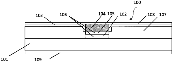
forming, on an upper surface of the multiplication layer and dielectric layer, at least one avalanche amplifier by etching a notch in both the dielectric layer and multiplication layer, wherein side walls of the notch are covered with a dielectric layer;
forming a contact layer of the at least one avalanche amplifier by (i) filling the notch with highly doped polycrystalline silicon with an opposite conductivity of the multiplication layer, then (ii) followed by diffusion of a dopant from the polycrystalline silicon area into the multiplication layer, wherein a photoconverter layer is formed outside the notch;
forming a first electrode made of a transparent material on surfaces of both the contact layer and dielectric layer; and
forming a second electrode on a bottom surface of the semiconductor wafer.
|