| CPC H01L 31/0735 (2013.01) | 11 Claims |
|
1. A photovoltaic device comprising:
a growth substrate;
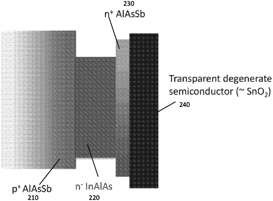
a heavily-doped p-type layer deposited on the growth substrate, wherein the p-type layer is doped at a dopant concentration greater than 1018 cm−3, wherein the p-type layer comprises an aluminum arsenic antimonide (AlAsSb) or an indium aluminum arsenide (InAlAs);
a lightly-doped n-type absorption layer deposited over the p-type layer and comprising a band structure that substantially matches the solar spectrum and comprising a plurality of valleys, wherein the absorption layer is doped at a dopant concentration of less than 1016 cm−3, wherein the absorption layer comprises an indium gallium arsenide (InGaAs) or an InAlAs;
a heavily-doped n-type carrier-collector layer deposited over the lightly-doped n-type absorption layer, wherein the carrier-collector layer is doped at a dopant concentration greater than 1018 cm−3, wherein the carrier-collector layer comprises an AlAsSb or an InAlAs and has a thickness less than a thickness of the absorption layer, wherein the carrier-collector layer further comprises a conduction band having a bottom, and wherein the bottom is substantially equal to an energy level of at least one upper valley of the plurality of valleys; and
a contact layer comprising a degenerate semiconductor material deposited on a surface of the carrier-collector layer, wherein the absorption layer has a thickness in a range of about 180 nanometers (nm) to about 220 nm.
|