| CPC H01L 31/052 (2013.01) [H01L 31/02168 (2013.01); H01L 31/022425 (2013.01)] | 8 Claims |
|
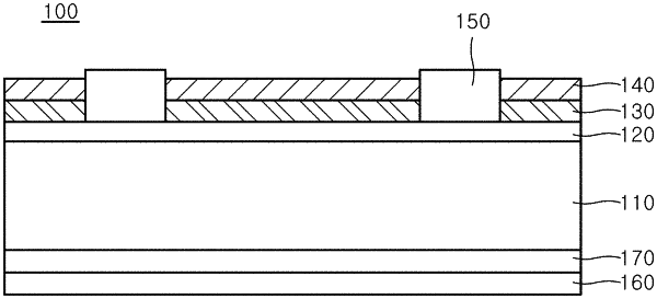
1. A solar cell comprising:
a semiconductor substrate;
an emitter layer disposed on one surface of the semiconductor substrate;
a planar cooling layer comprising a PDMS and disposed on one surface of the emitter layer;
an anti-reflection film disposed between the emitter layer and the planar cooling layer; and
a front surface electrode passing through the planar cooling layer and the anti-reflection film to be connected to the emitter layer,
wherein the planar cooling layer absorbs a far-infrared ray from irradiated sunlight and emits a wavelength of the absorbed far-infrared ray, and
wherein a thickness of the planar cooling layer is in a range from 5 μm to 150 μm.
|