| CPC H01L 31/0475 (2014.12) [E06B 9/386 (2013.01); H01L 31/02008 (2013.01); H01L 31/048 (2013.01); H01L 31/0465 (2014.12); H01L 31/0516 (2013.01); H02S 30/20 (2014.12); H05K 1/0213 (2013.01); H05K 1/181 (2013.01); E06B 9/24 (2013.01); E06B 2009/2476 (2013.01); H01L 31/1876 (2013.01); H02S 20/22 (2014.12); H02S 20/26 (2014.12)] | 20 Claims |
|
1. A solar cell module comprising:
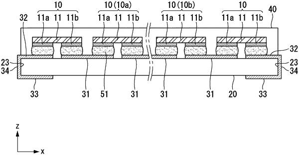
a PCB (Printed Circuit Board) substrate having a conductive pattern on a front surface and a rear surface thereof;
a plurality of solar cells mounted on the PCB substrate and arranged in a first direction, each of the plurality of solar cells including a first electrode and a second electrode arranged in parallel on a rear surface of a semiconductor substrate, wherein the first electrode and the second electrode are extended in the first direction, alternately arranged in a second direction crossing the first direction, and spaced apart from one another in the second direction,
wherein each of the plurality of solar cells is mounted so that the first and second electrodes face the conductive pattern, and the PCB substrate electrically connects the plurality of solar cells with each other; and
a protective film encapsulating the plurality of solar cells on the front surface of the PCB substrate,
wherein the conductive pattern includes:
a plurality of conductive portions, each of the plurality of conductive portions being arranged on the front surface of the PCB substrate and between two adjacent solar cells among the plurality of solar cells in a direction of a thickness of the solar cell module to electrically connect the two adjacent solar cells among the plurality of solar cells,
a terminal portion arranged on the front surface of the PCB substrate and adjacent to an outer conductive portion of the plurality of conductive portions, wherein the terminal portion is electrically connected to the outer conductive portion of the plurality of conductive portions by the semiconductor substrate of one of the plurality of solar cells,
an electrode portion formed on the rear surface of the PCB substrate, wherein the electrode portion forms an electrode for connecting the solar cell module to an external load, and
a connection portion proximate an outermost side surface of the PCB substrate, wherein the connection portion directly and electrically connects the terminal portion to the electrode portion of the conductive pattern,
wherein the PCB substrate comprises a groove portion recessed inwardly from the outermost side surface of the PCB substrate, wherein the front surface of the PCB substrate has a minimum width measured in the second direction that is defined by the groove portion, wherein the rear surface of the PCB substrate has a minimum width measured in the second direction that is defined by the groove portion,
wherein the connection portion is disposed in the groove portion, wherein an outermost surface of the connection portion is offset from the outermost side surface of the PCB substrate in the second direction such that the connection portion does not protrude from the outermost side surface of the PCB substrate,
wherein each of the plurality of solar cells and each of the plurality of conductive portions is a rectangular shape having a first side and a second side in the first direction,
wherein each of the plurality of conductive portions is disposed on the PCB substrate such that a first side of the conductive portion overlaps with a second side of a first solar cell and a second side of the conductive portion overlaps with a first side of a second solar cell, wherein the first and second solar cells are among the two adjacent solar cells in the first direction,
wherein the PCB substrate further comprises an insulating layer covering the plurality of conductive portions on the front surface of the PCB substrate, and
wherein the insulating layer includes a first contact hole to be disposed at a corresponding first side of the conductive portion and to expose the second electrode of the first solar cell and a second contact hole to be disposed at a corresponding second side of the conductive portion and to expose the first electrode of the second solar cell.
|