| CPC H01L 29/872 (2013.01) [H01L 29/0688 (2013.01); H01L 29/1608 (2013.01)] | 18 Claims |
|
1. A Junction Barrier Schottky (JBS) diode comprising:
a silicon carbide (SiC) substrate of a first conductivity type;
an epitaxial layer of the first conductivity type disposed above the SiC substrate and extending up to a top planar surface, the epitaxial layer including a plurality of Schottky barrier contact regions;
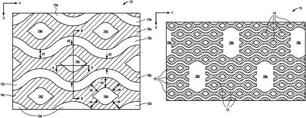
a plurality of first regions of a second conductivity type, the first regions being disposed in the epitaxial layer adjoining the top planar surface and extending downward to a depth, each of the first regions having a wave-shaped pattern across the top planar surface, the wave-shaped pattern extending in first and second lateral directions, each of the first regions being separated from an adjacent one of the first regions by one of the Schottky barrier contact regions;
a plurality of second regions of the second conductivity type each of which is laterally surrounded by a Schottky barrier contact region, each of the second regions being separated from an adjacent first region by a predetermined distance;
a top metal layer disposed along the top planar surface in direct contact with the Schottky barrier contact regions and the first and second regions, the top metal layer comprising an anode of the JBS diode;
a bottom metal layer disposed beneath the SiC substrate, the bottom metal layer comprising a cathode of the JBS diode; and
wherein the wave-shaped pattern comprise semi-circular regions that extend in the first and second lateral directions, with the semi-circular regions alternating orientation by 180 degrees along the second lateral direction.
|