| CPC H01L 29/78696 (2013.01) [H01L 21/8238 (2013.01); H01L 27/088 (2013.01); H01L 27/092 (2013.01); H01L 27/11807 (2013.01); H01L 29/06 (2013.01); H01L 29/0673 (2013.01); H01L 29/41733 (2013.01); H01L 29/42392 (2013.01); H01L 29/775 (2013.01); H01L 21/823412 (2013.01); H01L 21/823475 (2013.01); H01L 27/0207 (2013.01); H01L 27/1203 (2013.01); H01L 2027/11874 (2013.01)] | 16 Claims |
|
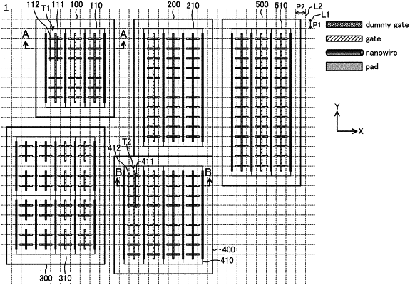
1. A semiconductor chip, comprising:
a first block including a standard cell having a first nanowire field effect transistor (FET); and
a second block including a second nanowire FET,
wherein
the first nanowire FET in the first block includes:
at least two first nanowires extending in a first direction;
a first pair of pads that are respectively arranged at both ends of the first nanowires in the first direction, and each connected to the first nanowires; and
a first gate electrode that extends in a second direction perpendicular to the first direction, and surrounds a periphery of the first nanowires within a predetermined range of the first nanowires in the first direction,
the first pair of pads are arranged at a first pitch in the first direction, and
the first nanowires are arranged at a second pitch in a third direction perpendicular to the first direction and the second direction;
the second nanowire FET in the second block includes:
at least two second nanowires extending in the first direction;
a second pair of pads that are respectively arranged at both ends of the second nanowires in the first direction, and each connected to the second nanowires; and
a second gate electrode that extends in the second direction, and surrounds a periphery of the second nanowires within a predetermined range of the second nanowires in the first direction,
the second pair of pads are arranged at the first pitch in the first direction, and
the second nanowires are arranged at the second pitch in the third direction.
|