| CPC H01L 29/785 (2013.01) [H01L 29/0649 (2013.01); H01L 29/41791 (2013.01); H01L 29/6681 (2013.01)] | 9 Claims |
|
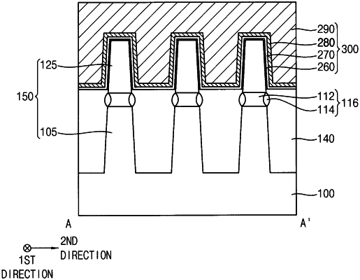
1. A semiconductor device, comprising:
an active pattern structure on a substrate, the active pattern structure comprising:
a lower active pattern protruding from an upper surface of the substrate in a vertical direction substantially perpendicular to the upper surface of the substrate;
an upper active pattern directly on the lower active pattern; and
a buffer between the lower active pattern and the upper active pattern, wherein the buffer contacts edge portions of the lower and upper active patterns and comprises aluminum silicon oxide;
an isolation pattern on the substrate, wherein the isolation pattern is on at least a portion of a sidewall of the active pattern structure;
a gate electrode structure on the active pattern structure; and
a source/drain layer on a portion of the active pattern structure adjacent the gate electrode structure.
|