| CPC H01L 29/7848 (2013.01) [H01L 21/02057 (2013.01); H01L 21/02532 (2013.01); H01L 21/324 (2013.01); H01L 29/045 (2013.01); H01L 29/0847 (2013.01); H01L 29/165 (2013.01); H01L 29/6656 (2013.01); H01L 29/66575 (2013.01); H01L 29/66636 (2013.01); H01L 29/7833 (2013.01); H01L 29/66628 (2013.01)] | 20 Claims |
|
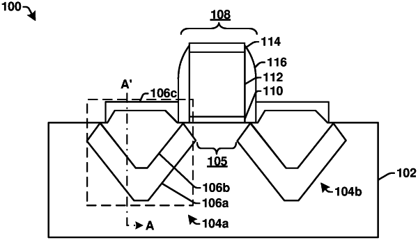
1. A method of forming a transistor device, comprising:
forming a gate structure onto a semiconductor substrate;
forming a source/drain recess within the semiconductor substrate adjacent to a side of the gate structure; and
forming a first strain inducing layer within the source/drain recess, wherein the first strain inducing layer comprises a strain inducing component with a strain inducing component concentration profile that continuously decreases from a bottommost surface of the first strain inducing layer to a position above the bottommost surface; and
forming a second strain inducing layer onto the first strain inducing layer, wherein the second strain inducing layer has a bottommost surface that faces the semiconductor substrate and that is below a top of the first strain inducing layer, and wherein the second strain inducing layer comprises a second inducing component concentration profile that increases from the bottommost surface of the second strain inducing layer to a position above the bottommost surface.
|
|
7. A method of forming a transistor device, comprising:
forming a gate structure onto a substrate;
forming a source/drain recess within the substrate next to the gate structure;
forming a first strain inducing layer onto a horizontally extending surface and sidewalls of the substrate that define the source/drain recess; and
forming a second strain inducing layer within the source/drain recess and onto a horizontally extending surface and along interior sidewalls of the first strain inducing layer that face one another, wherein the first strain inducing layer comprises a first strain inducing component with a first concentration profile that is discontinuous with a second concentration profile of a second strain inducing component within the second strain inducing layer.
|
|
16. A method of forming a transistor device, comprising:
forming a gate structure onto a substrate;
forming a source/drain recess within the substrate next to the gate structure;
forming a first strain inducing layer in the source/drain recess, wherein the first strain inducing layer has a first concentration profile that decreases as a distance from the substrate increases; and
forming a second strain inducing layer in the source/drain recess, wherein the second strain inducing layer has a second concentration profile that increases as a distance from the first strain inducing layer increases.
|