| CPC H01L 29/6681 (2013.01) [H01L 21/823431 (2013.01); H01L 29/7851 (2013.01)] | 15 Claims |
|
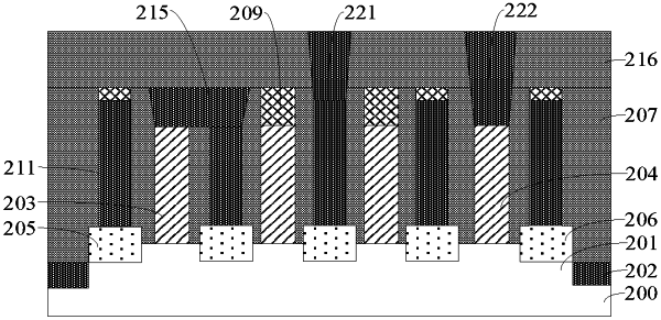
1. A semiconductor structure, comprising:
a substrate;
a first gate structure over the substrate;
a second gate structure over the substrate;
a protection layer formed on a top of the second gate structure;
a first source-drain doped layer formed between the first gate structure and the second gate structure;
a first dielectric layer formed on the substrate, covering a sidewall of the first gate structure and a sidewall of the second gate structure, and exposing a top surface of the protection layer;
a first conductive structure in the first dielectric layer over the first source-drain doped layer;
a conductive layer on the first gate structure and the first conductive structure, wherein a top surface of the conductive layer is coplanar with a top surface of the first dielectric layer;
a second source-drain doped layer, formed between the second gate structure and a third gate structure;
a second conductive structure, formed in the first dielectric layer over the second source-drain doped layer;
a second dielectric layer, formed over the first dielectric layer, the conductive layer, and the protection layer;
a source-drain plug formed in the second dielectric layer, extending into an inside of the first dielectric layer, and being in contact with a portion of the second conductive structure, a bottom surface of the source-drain plug being lower than the top surface of the conductive layer, and a top surface of the source-drain plug being higher than the top surface of the conductive layer; and
a gate plug, formed in the second dielectric layer, extending into an inside of the first dielectric layer, and being in contact with a portion of the third gate structure, a bottom surface of the gate plug being lower than the top surface of the conductive layer, and a top surface of the gate plug being higher than the top surface of the conductive layer;
wherein the second dielectric layer exposes top surfaces of the source-drain plug and the gate plug.
|