| CPC H01L 29/66666 (2013.01) [H01L 29/0692 (2013.01); H01L 29/0847 (2013.01); H01L 29/1037 (2013.01); H01L 29/7827 (2013.01); H01L 29/0653 (2013.01)] | 9 Claims |
|
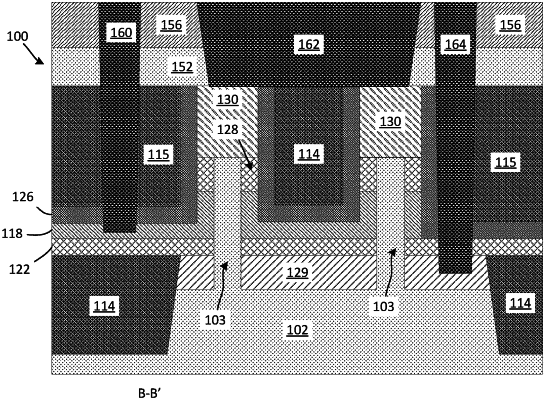
1. A semiconductor device comprising:
a bottom source/drain;
a top source/drain; and
a fin provided between the bottom source/drain and the top source/drain, the fin including a first fin structure and a second fin structure that vertically extend from a substrate, the vertical extending portions of the first and second fin structures spaced apart from each other, and that are symmetric to each other in a plan view,
wherein each of the first and second fin structures includes a main fin extending laterally in a first direction, and first and second extension fins extending laterally from the main fin in a second direction perpendicular to the first direction, and wherein the main fin extends laterally in the first direction beyond where the first and second extension fins connect to the main fin.
|