| CPC H01L 29/42364 (2013.01) [H01L 29/40111 (2019.08); H01L 29/40114 (2019.08); H01L 29/40117 (2019.08); H01L 29/7827 (2013.01); H10B 41/27 (2023.02); H10B 43/27 (2023.02); H10B 51/20 (2023.02)] | 9 Claims |
|
1. A method of forming a memory device, comprising:
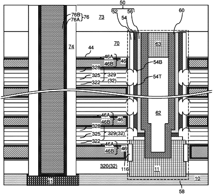
forming a vertical repetition of a unit layer stack, wherein the unit layer stack comprises a sacrificial material layer and a set of layers including, from bottom to top, a lower insulating sublayer, a first spacer-level sacrificial sublayer, a disposable material sublayer, a second spacer-level sacrificial sublayer, and an upper insulating sublayer;
forming memory openings through the vertical repetition;
forming memory opening fill structures in the memory openings, wherein each of the memory opening fill structures comprises a vertical semiconductor channel and a memory material layer;
forming a backside trench through the vertical repetition;
forming insulating-level backside recesses by removing the disposable material sublayers selective to materials of the sacrificial material layers, the lower insulating sublayers, the first spacer-level sacrificial sublayers, the second spacer-level sacrificial sublayers, and the upper insulating sublayers employing a first isotropic etch process;
removing the first spacer-level sacrificial sublayers and the second spacer-level sacrificial sublayers selective to the lower insulating sublayers and the upper insulating sublayers employing a second isotropic etch process, whereby the insulating-level backside recesses are expanded in volume;
depositing center insulating sublayers within the insulating-level backside recesses, wherein each contiguous combination of a lower insulating sublayer, an upper insulating sublayer, and a center insulating sublayer comprises a composite insulating layer, and wherein an alternating stack of composite insulating layers and the sacrificial material layers is formed; and
replacing the sacrificial material layers with electrically conductive layers after the step of depositing the center insulating sublayers.
|