| CPC H01L 29/4236 (2013.01) [H01L 29/0623 (2013.01); H01L 29/1083 (2013.01); H01L 29/66734 (2013.01); H01L 29/7813 (2013.01)] | 13 Claims |
|
1. A method for forming a shielding polysilicon sidewall for protecting a shielded gate trench metal-oxide-semiconductor field effect transistor (SGT MOSFET), comprising:
forming a heavily N-type doped semiconductor substrate with an N-type epitaxial layer to form an semiconductor N-type epitaxial substrate and forming a trench on a surface of the semiconductor N-type epitaxial substrate;
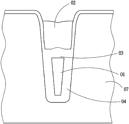
forming a liner oxide layer on an inner wall of the trench;
arranging a heavily N-type doped (>2e20/cm3) shielding polysilicon in the trench, the heavily N-type doped shielding polysilicon not being in contact with the source metal layer;
forming a transition oxide layer on a top and sidewall surface of the heavily N-type doped shielding polysilicon;
removing the liner oxide layer and the transition oxide layer from a top surface of the heavily N-type doped shielding polysilicon, while keeping some remaining transition oxide layer on the sidewall of the heavily N-type doped shielding polysilicon;
forming an inter-polysilicon oxide (IPO) layer on the top surface of the heavily N-type doped shielding polysilicon, the inner wall of the trench; and
forming an N-type doped gate polysilicon above the heavily N-type doped shielding polysilicon, the N-type doped gate polysilicon being isolated from the heavily N-type doped shielding polysilicon through the IPO layer.
|