US 11,749,733 B2
FIN shaping using templates and integrated circuit structures resulting therefrom
Leonard P. Guler, Hillsboro, OR (US); Biswajeet Guha, Hillsboro, OR (US); Mark Armstrong, Portland, OR (US); William Hsu, Hillsboro, OR (US); Tahir Ghani, Portland, OR (US); and Swaminathan Sivakumar, Beaverton, OR (US)
Assigned to Intel Corporation, Santa Clara, CA (US)
Filed by Intel Corporation, Santa Clara, CA (US)
Filed on Mar. 10, 2022, as Appl. No. 17/691,926.
Application 17/691,926 is a continuation of application No. 16/772,631, granted, now 11,302,790, previously published as PCT/US2018/019456, filed on Feb. 23, 2018.
Prior Publication US 2022/0199792 A1, Jun. 23, 2022
This patent is subject to a terminal disclaimer.
Int. Cl. H01L 29/417 (2006.01); H01L 27/088 (2006.01); H01L 29/16 (2006.01); H01L 29/20 (2006.01); H01L 29/78 (2006.01)
CPC H01L 29/41791 (2013.01) [H01L 27/0886 (2013.01); H01L 29/16 (2013.01); H01L 29/20 (2013.01); H01L 29/785 (2013.01)] 22 Claims
OG exemplary drawing
 
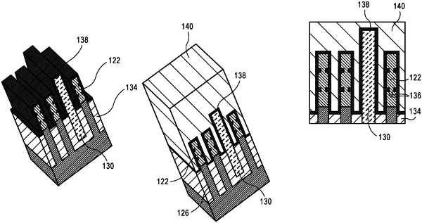
1. An integrated circuit structure, comprising:
a semiconductor fin having a protruding fin portion above an isolation structure, the protruding fin portion having a vertical portion and one or more lateral recess pairs in the vertical portion, and the vertical portion comprising a same semiconductor material continuous from a location above the one or more lateral recess pairs to a location below the one or more lateral recess pairs;
a gate stack over and conformal with the protruding fin portion of the semiconductor fin;
a first source or drain region at a first side of the gate stack; and
a second source or drain region at a second side of the gate stack opposite the first side of the gate stack.