| CPC H01L 29/41775 (2013.01) [H01L 29/4238 (2013.01); H01L 23/34 (2013.01); H01L 23/4951 (2013.01); H01L 23/49562 (2013.01); H01L 23/49568 (2013.01); H01L 24/33 (2013.01); H01L 24/73 (2013.01); H01L 29/0696 (2013.01); H01L 29/41741 (2013.01); H01L 2224/33181 (2013.01); H01L 2224/73215 (2013.01); H01L 2224/73265 (2013.01); H01L 2924/10253 (2013.01); H01L 2924/10272 (2013.01)] | 18 Claims |
|
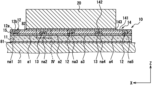
1. A semiconductor device comprising:
a semiconductor chip having a front surface and a back surface opposite to the front surface;
a first conductive member disposed adjacent to the back surface of the semiconductor chip; and
a second conductive member disposed adjacent to the front surface of the semiconductor chip, wherein
the semiconductor chip includes:
a semiconductor substrate having a plurality of active regions formed with elements, and an inactive region not formed with an element, the inactive region including an inter-inactive portion disposed between at least two active regions and an outer peripheral inactive portion disposed on an outer periphery of the at least two active regions;
a surface electrode disposed to continuously extend above the at least two active regions and the inter-inactive portion; and
a plurality of gate wirings disposed above the inactive region adjacent to the front surface, the plurality of gate wirings including a first gate wiring disposed on an outer periphery of the surface electrode, and a second gate electrode disposed at a position facing the surface electrode, and
the first gate wiring includes a polysilicon wiring and a metal wiring, and
the second gate wiring includes a polysilicon wiring without having a metal wiring.
|