| CPC H01L 29/404 (2013.01) [H01L 29/2003 (2013.01); H01L 29/402 (2013.01); H01L 29/66462 (2013.01); H01L 29/778 (2013.01); H01L 29/7786 (2013.01)] | 33 Claims |
|
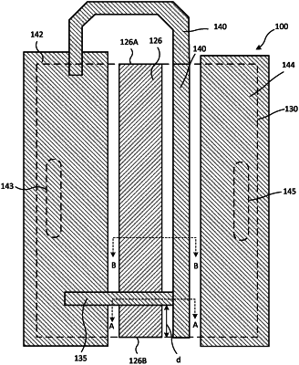
33. A transistor device, comprising:
a semiconductor layer;
source and drain contacts on the semiconductor layer;
a gate contact on the semiconductor layer between the source and drain contacts;
a field plate over the semiconductor layer between the gate contact and the drain contact;
a source metallization in electrical contact with the source contact by a conductive via;
a first electrical connection between the field plate and the source metallization, wherein the first electrical connection is outside an active region of the transistor device; and
a second electrical connection between the field plate and the source metallization that is within the active region of the device.
|