| CPC H01L 29/1608 (2013.01) [H01L 29/32 (2013.01); H01L 29/66068 (2013.01); H01L 29/7802 (2013.01)] | 11 Claims |
|
1. A semiconductor device, comprising:
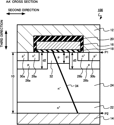
a silicon carbide layer having a first face and a second face facing the first face and including:
a first silicon carbide region of a first conductive type;
a second silicon carbide region of a second conductive type disposed between the first silicon carbide region and the first face;
a third silicon carbide region of a second conductive type disposed between the first silicon carbide region and the first face, the first silicon carbide region being interposed between the second silicon carbide region and the third silicon carbide region;
a fourth silicon carbide region of a first conductive type disposed between the second silicon carbide region and the first face;
a fifth silicon carbide region of a first conductive type disposed between the third silicon carbide region and the first face;
a sixth silicon carbide region of a second conductive type disposed between the first silicon carbide region and the first face and disposed between the second silicon carbide region and the third silicon carbide region; and
a crystal defect, at least a part of the crystal defect being disposed in the sixth silicon carbide region;
a gate electrode disposed on a side of the first face of the silicon carbide layer;
a gate insulating layer disposed between the second silicon carbide region and the gate electrode, between the third silicon carbide region and the gate electrode, and between the sixth silicon carbide region and the gate electrode;
a first electrode disposed on a side of the first face of the silicon carbide layer; and
a second electrode disposed on a side of the second face of the silicon carbide layer.
|