| CPC H01L 29/0653 (2013.01) [H01L 21/763 (2013.01); H01L 21/76264 (2013.01); H01L 21/76283 (2013.01); H01L 21/823481 (2013.01); H01L 29/1095 (2013.01); H01L 29/66681 (2013.01); H01L 29/7816 (2013.01); H01L 29/7841 (2013.01)] | 20 Claims |
|
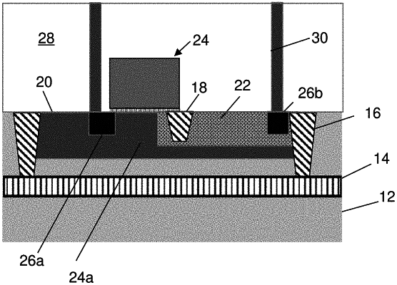
1. A structure comprising:
a first well in a semiconductor substrate, the first well extending between a deep trench isolation structure on both sides of a gate structure;
a second well in the semiconductor substrate, the second well comprising a dopant different than the first well and extending on one side of the gate structure within the first well;
a shallow trench isolation structure within the second well;
a drift region within the second well;
a source implant in the first well; and
a drain implant in a drift region within the second well and being remotely positioned from the shallow trench isolation structure.
|