| CPC H01L 29/0638 (2013.01) [H01L 27/0716 (2013.01); H01L 29/36 (2013.01); H01L 29/66333 (2013.01); H01L 29/66348 (2013.01); H01L 29/7395 (2013.01); H01L 29/7397 (2013.01); H01L 29/861 (2013.01); H01L 21/02236 (2013.01); H01L 21/266 (2013.01); H01L 21/26513 (2013.01); H01L 21/304 (2013.01); H01L 21/324 (2013.01); H01L 27/0664 (2013.01)] | 13 Claims |
|
1. An insulated gate bipolar transistor (IGBT), comprising:
a heavily doped semiconductor layer;
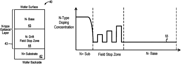
an epitaxial layer of a first conductivity type formed on the semiconductor layer, the epitaxial layer including a first portion of the first conductivity type adjacent to the semiconductor layer forming a field stop zone, and the epitaxial layer further including a second portion of the first conductivity type forming a base region, the field stop zone having a first side adjacent to the semiconductor layer and a second side adjacent to the base region, the base region having a first side adjacent to the field stop zone and a second side opposite the first side, the field stop zone and the base region being formed using a same dopant of the first conductivity type;
a device region formed in the second side of the base region, the device region comprising a PN junction; and
a gate dielectric layer and a conductive gate formed in or on the epitaxial layer at the second side of the base region,
wherein the epitaxial layer has a first doping level as a background doping level and has multiple doped regions with step increase in doping levels from the first doping level and being formed spaced apart within the field stop zone, each of the doped regions being formed using the same dopant of the first conductivity type as the field stop zone and having a peak doping level, and a first doped region adjacent to the first side of the field stop zone has a first peak doping level that is not higher than a last peak doping level of a last doped region adjacent to the base region, and the thickness of the first doped region is less than a thickness of the last doped region, and wherein the base region has a constant doping level and the background doping level is higher than or the same as the constant doping level of the base region.
|