| CPC H01L 28/60 (2013.01) [H01L 28/56 (2013.01); H10B 53/30 (2023.02); H01L 21/02197 (2013.01); H01L 21/02266 (2013.01)] | 15 Claims |

|
1. A method of manufacturing a capacitor, the method comprising:
forming a lower electrode having a perovskite structure;
forming a first dielectric layer, including a perovskite structure, on the lower electrode, the first dielectric layer having a first dielectric constant and a first band gap energy;
forming a second dielectric layer, including a perovskite structure, on the first dielectric layer, the second dielectric layer having a second dielectric constant less than the first dielectric constant and a second band gap energy greater than the first band gap energy; and
forming an upper electrode having a perovskite structure on the second dielectric layer,
wherein a degree of a lattice mismatch between the lower electrode and the first dielectric layer is about 5% or less and a degree of a lattice mismatch between the lower electrode and the second dielectric layer is about 5% or less,
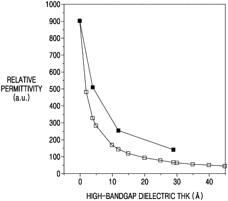
wherein a ratio of a thickness of the second dielectric layer to a total thickness of the first dielectric layer and the second dielectric layer is about 30% or less, and
wherein the degree of lattice mismatch between the lower electrode and the first dielectric layer is less than the degree of lattice mismatch between the lower electrode and the second dielectric layer.
|