| CPC H01L 28/60 (2013.01) [H01L 24/48 (2013.01); H01L 24/85 (2013.01); H01L 2224/48265 (2013.01); H01L 2924/19104 (2013.01)] | 19 Claims |
|
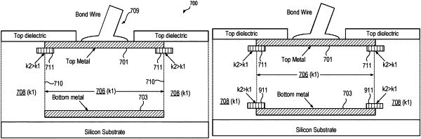
1. An integrated circuit comprising:
a bottom conductive plate;
a top conductive plate;
a first dielectric region formed from a first dielectric material, a first portion of the first dielectric region being between the top conductive plate and the bottom conductive plate;
a second dielectric region that includes a second dielectric material having a higher dielectric constant than the first dielectric material, the second dielectric region having an inner portion below a portion of the top conductive plate and an outer portion extending beyond an edge of the top conductive plate; and
a third dielectric region that includes the second dielectric material, the third dielectric region having an inner portion above a portion of the bottom conductive plate and an outer portion extending beyond an outer edge of the bottom conductive plate.
|
|
9. A method of making an integrated circuit comprising:
forming a bottom conductive plate;
forming a first dielectric region of at least a first dielectric material, a first portion of the first dielectric region being formed above the bottom conductive plate;
forming a second dielectric region having an inner perimeter and an outer perimeter, the second dielectric region being formed above the first portion of the first dielectric region, the second dielectric region including at least a second dielectric material, the second dielectric material having a higher dielectric constant than the first dielectric material; and
forming a top conductive plate such that an outer portion of the second dielectric region extends beyond an edge of the top conductive plate and an inner portion of the top conductive plate is above and adjacent to an inner portion of the second dielectric region; and
forming a third dielectric region that includes the second dielectric material, the third dielectric region having a second inner perimeter and a second outer perimeter, a portion of a bottom surface of the third dielectric region being formed adjacent to a top surface of the bottom conductive plate.
|
|
16. A method of making an integrated circuit comprising:
forming a bottom conductive plate;
forming a first dielectric region of at least a first dielectric material, a first portion of the first dielectric region being formed above the bottom conductive plate;
forming a second dielectric region having an inner perimeter and an outer perimeter, the second dielectric region being formed above the first portion of the first dielectric region, the second dielectric region including at least a second dielectric material, the second dielectric material having a higher dielectric constant than the first dielectric material; and
forming a top conductive plate such that an outer portion of the second dielectric region extends beyond an edge of the top conductive plate and an inner portion of the top conductive plate is above and adjacent to an inner portion of the second dielectric region;
forming a layer that includes the second dielectric material above the first dielectric region;
removing a first portion of the layer to form the second dielectric region; and
forming the top conductive plate with a portion of the top conductive plate being formed in a region where the first portion of the layer was removed.
|