| CPC H01L 27/15 (2013.01) [H01L 33/405 (2013.01); H01L 33/62 (2013.01); H01L 27/153 (2013.01); H01L 33/0016 (2013.01); H01L 33/38 (2013.01); H01L 2933/0066 (2013.01)] | 17 Claims |
|
1. A light emitting diode, comprising:
a first conductivity type semiconductor layer;
a mesa disposed on the first conductivity type semiconductor layer, the mesa comprising an active layer and a second conductivity type semiconductor layer;
an ohmic layer disposed on the mesa and electrically connected to the second conductivity type semiconductor layer;
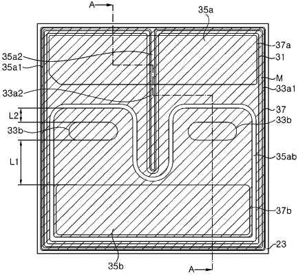
a lower insulation layer covering the mesa and the ohmic layer, the lower insulation layer comprising a first opening configured to expose the first conductivity type semiconductor layer and a second opening configured to expose the ohmic layer;
a first pad metal layer disposed on the lower insulation layer and electrically connected to the first conductivity type semiconductor layer through the first opening;
a second pad metal layer disposed on the lower insulation layer, and electrically connected to the ohmic layer through the second opening;
an upper insulation layer covering the first pad metal layer and the second pad metal layer, the upper insulation layer comprising a first opening configured to expose the first pad metal layer and a plurality of second openings configured to expose the second pad metal layer;
a first bump pad connected to the first pad metal layer through the first opening of the upper insulation layer; and
a second bump pad connected to the second pad metal layer through the plurality of second openings of the upper insulation layer,
wherein the plurality of second openings of the upper insulation layer are separated from the second opening of the lower insulation layer not to overlap each other, and
wherein the second opening of the lower insulation layer has an oval shape,
wherein the lower insulation layer comprises a plurality of second openings, and
a shortest distance from one of the second openings of the lower insulation layer to one of the second openings of the upper insulation layer is greater than a shortest distance between the second openings of the lower insulation layer.
|