| CPC H01L 27/14665 (2013.01) [H01L 27/1463 (2013.01); H01L 27/14609 (2013.01); H01L 27/14621 (2013.01); H04N 25/77 (2023.01)] | 17 Claims |
|
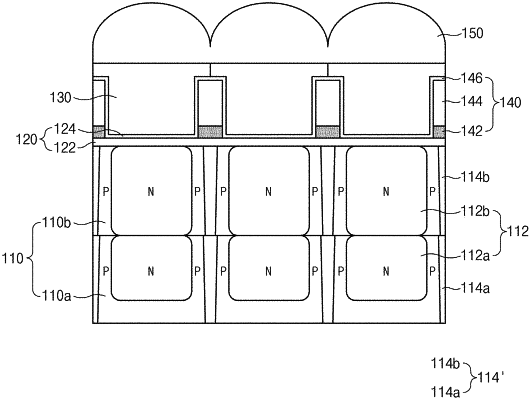
1. A method for forming an image sensing device, comprising:
forming a first photoelectric conversion element in a first substrate by implanting first-type impurities into the first substrate;
providing a second substrate over the first substrate; and
forming a second photoelectric conversion element in the second substrate by implanting the first-type impurities into the second substrate, the second photoelectric conversion element being in contact with the first photoelectric conversion element,
wherein the first photoelectric conversion element and the second photoelectric conversion element form a single photoelectric conversion element by contacting each other.
|