| CPC H01L 27/14636 (2013.01) [H01L 24/05 (2013.01); H01L 27/14623 (2013.01); H01L 27/14685 (2013.01); H01L 24/06 (2013.01); H01L 27/14621 (2013.01); H01L 27/14634 (2013.01); H01L 2224/05025 (2013.01); H01L 2224/05082 (2013.01); H01L 2224/05184 (2013.01); H01L 2224/05186 (2013.01); H01L 2224/05624 (2013.01); H01L 2224/06181 (2013.01)] | 20 Claims |
|
1. An image sensor, comprising:
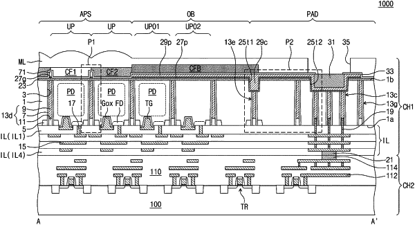
a substrate including a pixel region and a pad region and having a first surface and a second surface opposite to the first surface, wherein the pixel region of the substrate is provided with a plurality of unit pixels;
a first recess provided in the pad region of the substrate, wherein the first recess is recessed to a first depth from the second surface toward the first surface, and wherein a bottom surface of the first recess is lower than the second surface of the substrate;
an interlayer insulating layer disposed on the first surface;
an interconnection line disposed in the interlayer insulating layer;
a conductive pad disposed in the first recess of the pad region;
a plurality of penetration structures disposed in the pad region of the substrate and extending from the bottom surface of the first recess to the first surface of the substrate, and electrically connecting the conductive pad to the interconnection line; and
a deep device isolation structure disposed in the pixel region of the substrate, and extending from the second surface of the substrate to the first surface of the substrate to separate two adjacent unit pixels of the plurality of unit pixels from each other, wherein an upper surface of the deep device isolation structure is higher than an upper surface of each penetration structure of the plurality of penetration structures.
|