| CPC H01L 27/14605 (2013.01) [H01L 21/76898 (2013.01); H01L 23/481 (2013.01); H01L 27/1463 (2013.01); H01L 27/1464 (2013.01); H01L 27/14603 (2013.01); H01L 27/14607 (2013.01); H01L 27/14636 (2013.01); H01L 27/14641 (2013.01); H01L 27/14689 (2013.01); H01L 27/14643 (2013.01)] | 20 Claims |
|
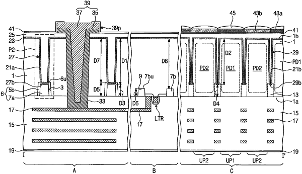
1. An image sensor, comprising:
a semiconductor substrate comprising a pad zone and having a first surface and a second surface opposing each other;
a first pad separation pattern on the pad zone and extending from the first surface of the semiconductor substrate toward the second surface of the semiconductor substrate;
a second pad separation pattern on the pad zone and extending from the second surface of the semiconductor substrate toward the first surface of the semiconductor substrate, wherein the second pad separation pattern is in contact with the first pad separation pattern; and
a through via on the pad zone and spaced apart from the first and second pad separation patterns, the through via penetrating the semiconductor substrate.
|