| CPC H01L 27/1259 (2013.01) [H01L 21/0214 (2013.01); H01L 21/0217 (2013.01); H01L 21/0228 (2013.01); H01L 21/02164 (2013.01)] | 15 Claims |
|
1. A manufacturing method of an array substrate, comprising:
providing a substrate;
depositing and patterning a gate layer on the substrate;
depositing a protective layer on the substrate covered with the gate layer by atomic layer deposition; and
depositing and patterning an amorphous silicon layer and an ohmic contact layer on the protective layer;
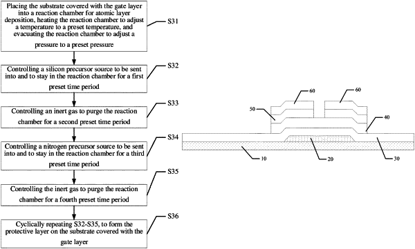
wherein depositing a protective layer on the substrate covered with the gate layer by atomic layer deposition comprises:
placing the substrate covered with the gate layer into a reaction chamber for atomic layer deposition, heating the reaction chamber to adjust a temperature to a preset temperature, and evacuating the reaction chamber to adjust a pressure to a preset pressure;
controlling a silicon precursor source to be sent into and to stay in the reaction chamber for 0.03 s-0.08 s;
controlling an inert gas to purge the reaction chamber for 5 s-10 s;
controlling a nitrogen precursor source to be sent into and to stay in the reaction chamber for a 18 s-30 s;
controlling the inert gas to purge the reaction chamber for 15 s-28 s; and
cyclically repeating the operations of controlling a silicon precursor source to be sent into and to stay in the reaction chamber for 0.03 s-0.08 s, controlling an inert gas to purge the reaction chamber for 5 s-10 s, controlling a nitrogen precursor source to be sent into and to stay in the reaction chamber for 18 s-30 s, and controlling the inert gas to purge the reaction chamber for 15 s-28 s, to form the protective layer on the substrate covered with the gate layer.
|