| CPC H01L 27/1244 (2013.01) [H01L 27/1259 (2013.01)] | 19 Claims |
|
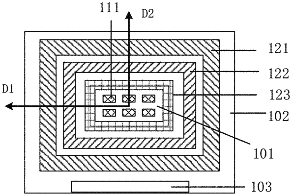
5. An electronic device substrate, comprising a base substrate, a first insulating layer, a plurality of light-emitting sub-units, a first conductive member, a second conductive member, and a third conductive member,
wherein the plurality of light-emitting sub-units are in an array region of the electronic device substrate, the first conductive member is in a periphery region, surrounding the array region, of the electronic device substrate, and the second conductive member is between the first conductive member and the array region;
each of the plurality of light-emitting sub-units comprises a first driving electrode and a second driving electrode, and the first driving electrode and the second driving electrode are configured to apply a light-emitting driving voltage;
the third conductive member is on the side of the first insulating layer away from the base substrate;
the third conductive member surrounds the array region, and the second conductive member surrounds the third conductive member;
each of the plurality of light-emitting sub-units comprises a light-emitting layer, and light-emitting layers of the plurality of light-emitting sub-units are integrated to form a light-emitting material layer; and
the light-emitting material layer extends onto the third conductive member and at least partially overlaps with the third conductive member.
|