| CPC H01L 27/1244 (2013.01) [G02F 1/1345 (2013.01); G02F 1/13458 (2013.01); G02F 1/133305 (2013.01); H01L 27/1218 (2013.01); H01L 27/1225 (2013.01); H01L 27/1248 (2013.01); G02F 1/133345 (2013.01); G02F 1/136286 (2013.01); G02F 2201/50 (2013.01); G09G 2300/0426 (2013.01); H01L 21/76895 (2013.01); H05B 45/60 (2020.01); H10K 59/00 (2023.02); H10K 59/124 (2023.02); H10K 59/131 (2023.02); H10K 77/111 (2023.02); H10K 2102/311 (2023.02); H10K 2102/341 (2023.02)] | 21 Claims |
|
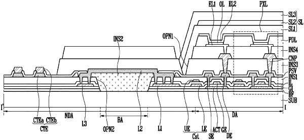
1. A display device, comprising:
a substrate including a display area and a non-display area;
a plurality of pixels provided in the display area;
a first insulating layer disposed on the substrate and having a removed area in a bending area of the non-display area;
a second insulating layer overlapping with the removed area of the first insulating layer;
first lines disposed on the substrate and electrically connected to the plurality of pixels; and
second lines disposed on the second insulating layer and electrically connected to the first lines,
wherein the second lines extend from an overlapping area in which the first lines overlap with the second lines to the bending area,
wherein the first insulating layer is an inorganic material and the second insulating layer is an organic material.
|