| CPC H01L 27/124 (2013.01) [G02F 1/136222 (2021.01); G02F 1/136295 (2021.01); H01L 27/1288 (2013.01)] | 16 Claims |
|
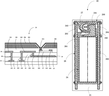
1. An array substrate, comprising:
a substrate;
a first metal layer disposed on the substrate and comprising a first data line and a first vertical scan line;
a first insulating layer disposed on the substrate and the first metal layer and covering the first metal layer;
a second metal layer disposed on the first insulating layer and comprising a horizontal scan line;
a second insulating layer disposed on the first insulating layer and the second metal layer and covering the second metal layer;
a first via hole and a second via hole penetrating the first insulating layer and the second insulating layer on the first metal layer;
a third via hole penetrating the second insulating layer; and
a third metal layer disposed on the second insulating layer and comprising a second data line and a second vertical scan line, wherein the second data line is connected in parallel with the first data line through the first via hole, the second vertical scan line is connected in parallel with the first vertical scan line through the second via hole, and the second vertical scan line is connected to the horizontal scan line through the third via hole;
wherein the first via hole, the second via hole, and the third via hole are formed by a same manufacturing process.
|