| CPC H01L 27/1225 (2013.01) [H01L 21/02554 (2013.01); H01L 21/02565 (2013.01); H01L 21/02631 (2013.01); H01L 27/1266 (2013.01); H01L 29/1033 (2013.01); H01L 29/24 (2013.01); H01L 29/66742 (2013.01); H01L 29/66969 (2013.01); H01L 29/7869 (2013.01); H01L 29/78606 (2013.01)] | 10 Claims |
|
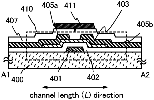
1. A semiconductor device comprising:
a substrate;
a pixel portion over the substrate; and
a driver circuit portion over the substrate,
wherein the pixel portion comprises a display element,
wherein the driver circuit portion comprises:
a conductive layer;
a first semiconductor layer and a second semiconductor layer arranged in a first direction;
an insulating layer between the conductive layer and each of the first semiconductor layer and the second semiconductor layer;
a source electrode layer electrically connected to the first semiconductor layer and the second semiconductor layer; and
a drain electrode layer electrically connected to the first semiconductor layer and the second semiconductor layer,
wherein a part of the first semiconductor layer is included in a first transistor and a part of the second semiconductor layer is included in a second transistor,
wherein a part of the conductive layer is included in the first transistor and a part of the conductive layer is included in the second transistor,
wherein the conductive layer extends beyond both side edges of the first semiconductor layer in the first direction, the first direction being the same as a channel width direction of the first transistor,
wherein the conductive layer extends beyond both side edges of the second semiconductor layer in the first direction, a channel width direction of the second transistor being the same as the first direction,
wherein the source electrode layer extends beyond the both side edges of the first semiconductor layer,
wherein the source electrode layer extends beyond the both side edges of the second semiconductor layer,
wherein the drain electrode layer extends beyond the both side edges of the first semiconductor layer,
wherein the drain electrode layer extends beyond the both side edges of the second semiconductor layer,
wherein the conductive layer includes a first region overlapping with a channel formation region of the first transistor, a second region overlapping with a channel formation region of the second transistor, and a third region not overlapping with neither the channel formation region of the first transistor nor the channel formation region of the second transistor, and
wherein, in a second direction perpendicular to the first direction, a width of the conductive layer in the third region is broader than a width of the conductive layer in the first region and a width of the conductive layer in the second region.
|