| CPC H01L 27/1225 (2013.01) [G09G 3/20 (2013.01); G09G 3/3674 (2013.01); G09G 3/3677 (2013.01); G11C 19/28 (2013.01); G11C 19/287 (2013.01); H01L 27/124 (2013.01); H01L 29/7869 (2013.01); G09G 2310/0286 (2013.01)] | 2 Claims |
|
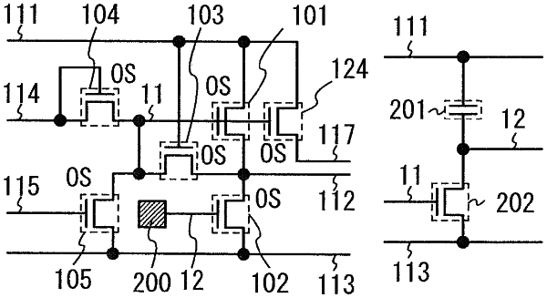
1. A semiconductor device comprising:
a first transistor;
a second transistor;
a third transistor;
a fourth transistor;
a fifth transistor;
a sixth transistor;
a seventh transistor; and
an eighth transistor,
wherein the first to eighth transistors have the same conductivity type,
wherein one of a source and a drain of the first transistor is electrically connected to a first line and the other of the source and the drain of the first transistor is electrically connected to a second line,
wherein one of a source and a drain of the second transistor is electrically connected to the second line and the other of the source and the drain of the second transistor is electrically connected to a third line,
wherein one of a source and a drain of the third transistor is electrically connected to a gate of the first transistor, the other of the source and the drain of the third transistor is electrically connected to the third line, and a gate of the third transistor is electrically connected to a gate of the second transistor,
wherein one of a source and a drain of the fourth transistor is electrically connected to the gate of the first transistor, the other of the source and the drain of the fourth transistor is electrically connected to a fourth line, and a gate of the fourth transistor is electrically connected to a fifth line,
wherein one of a source and a drain of the fifth transistor is electrically connected to the gate of the first transistor, the other of the source and the drain of the fifth transistor is electrically connected to the third line, and a gate of the fifth transistor is electrically connected to a sixth line,
wherein one of a source and a drain of the sixth transistor is electrically connected to the gate of the second transistor, the other of the source and the drain of the sixth transistor is electrically connected to the third line, and a gate of the sixth transistor is electrically connected to the gate of the first transistor,
wherein one of a source and a drain of the seventh transistor is electrically connected to the first line, the other of the source and the drain of the seventh transistor is electrically connected to a seventh line, and a gate of the seventh transistor is electrically connected to the gate of the first transistor,
wherein one of a source and a drain of the eighth transistor is electrically connected to the second line, the other of the source and the drain of the eighth transistor is electrically connected to the third line, and a gate of the eighth transistor is electrically connected to the sixth line,
wherein the ratio of the channel width to the channel length of the third transistor is smaller than the ratio of the channel width to the channel length of the fourth transistor,
wherein the second line serves as a first gate signal line,
wherein the fourth line serves as a second gate signal line,
wherein the sixth line serves as a third gate signal line, and
wherein the fourth line is configured to be supplied with a different signal from the fifth line.
|