| CPC H01L 27/0928 (2013.01) [G09G 3/32 (2013.01); H01L 27/06 (2013.01); H01L 29/0611 (2013.01); H04N 9/3123 (2013.01); H04N 9/3155 (2013.01); H05B 45/30 (2020.01); H10B 10/18 (2023.02); G09G 3/001 (2013.01); G09G 2330/12 (2013.01); H01L 29/78 (2013.01); H01L 29/8611 (2013.01)] | 13 Claims |
|
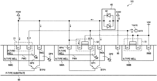
1. A circuit device comprising:
a first N-type well on a P-type substrate;
a first P-type well that is provided in the first N-type well, wherein a first ground power supply voltage is supplied to the first P-type well;
a first circuit element provided in the first P-type well;
a second N-type well on the P-type substrate;
a second P-type well that is provided in the second N-type well, wherein a power supply voltage different from the first ground power supply voltage is supplied to the second P-type well; and
a second circuit element provided in the second P-type well,
wherein the first ground power supply voltage or a first potential that is (i) greater than or equal to the potential of the first ground power supply voltage and (ii) less than the potential of a high potential-side power supply voltage supplied to a node of the circuit device is supplied to the first N-type well from a node that is not electrically connected to the node of the high potential-side power supply voltage,
a second ground power supply voltage different from the first ground power supply voltage is supplied to the second P-type well; and
a coupling circuit provided between the first ground power supply voltage and the second ground power supply voltage.
|