US 11,749,680 B2
Multi-threshold voltage non-planar complementary metal-oxide-semiconductor devices
Ruqiang Bao, Niskayuna, NY (US); and Koji Watanabe, Yokohama (JP)
Assigned to INTERNATIONAL BUSINESS MACHINES CORPORATION, Armonk, NY (US)
Filed by INTERNATIONAL BUSINESS MACHINES CORPORATION, Armonk, NY (US)
Filed on Dec. 2, 2022, as Appl. No. 18/61,149.
Application 17/481,497 is a division of application No. 16/573,348, filed on Sep. 17, 2019, granted, now 11,189,616.
Application 18/061,149 is a continuation of application No. 17/481,497, filed on Sep. 22, 2021, granted, now 11,605,634.
Prior Publication US 2023/0094258 A1, Mar. 30, 2023
This patent is subject to a terminal disclaimer.
Int. Cl. H01L 27/092 (2006.01); H01L 29/78 (2006.01); H01L 29/66 (2006.01); H01L 21/02 (2006.01); H01L 29/06 (2006.01)
CPC H01L 27/0922 (2013.01) [H01L 21/02178 (2013.01); H01L 27/0924 (2013.01); H01L 29/0665 (2013.01); H01L 29/66666 (2013.01); H01L 29/66795 (2013.01); H01L 29/785 (2013.01); H01L 29/7827 (2013.01)] 20 Claims
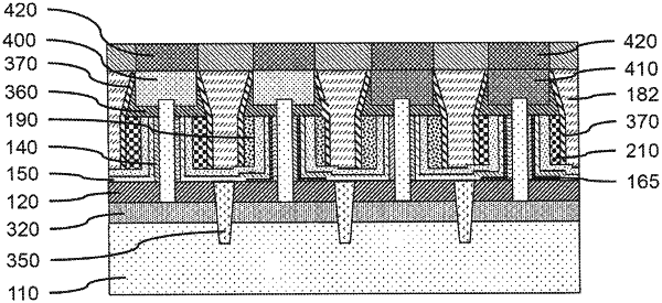
OG exemplary drawing
 
1. A method of fabricating a plurality of field effect transistor devices, comprising:
forming conversion layer segments on a gate dielectric layer on a subset of a plurality of semiconductor device channels;
forming a capping layer on each of the plurality of semiconductor device channels; and
heat treating the conversion layer segments and plurality of semiconductor device channels to form a dipole layer between an interfacial layer on the plurality of semiconductor device channels and gate dielectric layer on the subset of the plurality of semiconductor device channels.