| CPC H01L 27/088 (2013.01) [H01L 29/0649 (2013.01); H01L 29/7827 (2013.01)] | 20 Claims |
|
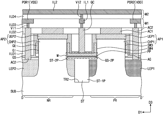
1. A method of fabricating a semiconductor device, the method comprising:
forming an active pattern on a substrate by patterning the substrate, the active pattern protruding above the substrate;
forming a device isolation layer on the substrate, the device isolation layer surrounding a first portion of the active pattern;
forming a gate electrode layer on the device isolation layer and the active pattern, the gate electrode layer including a vertical portion that vertically extends along a sidewall of the active pattern;
forming a spacer on the vertical portion of the gate electrode layer;
forming a void below the vertical portion of the gate electrode layer by selectively removing a lower portion of the gate electrode layer;
forming a gate spacer on the vertical portion of the gate electrode layer, the gate spacer defining an air gap by not filling the void; and
forming an upper epitaxial pattern on the active pattern.
|