| CPC H01L 27/0629 (2013.01) [H01L 27/0658 (2013.01); H01L 29/7395 (2013.01); H01L 29/7397 (2013.01); H01L 29/7815 (2013.01); H01L 29/0696 (2013.01); H01L 29/0878 (2013.01); H01L 29/1095 (2013.01); H01L 29/4236 (2013.01); H01L 29/7827 (2013.01)] | 5 Claims |
|
1. A semiconductor device that detects current in a main insulated-gate semiconductor device element by a potential difference, the semiconductor device, comprising:
the main insulated-gate semiconductor device element;
a current-detecting insulated-gate semiconductor device element having a size smaller than a size of the main insulated-gate semiconductor device element; and
a resistor connected between the main insulated-gate semiconductor device element and the current-detecting insulated-gate semiconductor device element, the resistor having the potential difference between ends thereof, wherein
the current-detecting insulated-gate semiconductor device element, under reverse bias, has a breakdown voltage higher than a breakdown voltage of the main insulated-gate semiconductor device element under reverse bias,
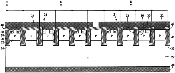
the main insulated-gate semiconductor device element has:
a first first-conductivity-type semiconductor layer having a first main surface and a second main surface opposite to each other,
a first second-conductivity-type semiconductor region provided in the first first-conductivity-type semiconductor layer at the first main surface,
a first first-conductivity-type high-concentration semiconductor region selectively provided in the first second-conductivity-type semiconductor region at a surface of the first second-conductivity-type semiconductor region,
a first gate electrode provided, via a first gate insulating film, in a first trench that penetrates the first first-conductivity-type high-concentration semiconductor region and the first second-conductivity-type semiconductor region and reaches the first first-conductivity-type semiconductor layer,
a first electrode in contact with the first first-conductivity-type high-concentration semiconductor region and the first second-conductivity-type semiconductor region, and
a second electrode provided facing the second main surface of the first first-conductivity-type semiconductor layer, and
the current-detecting insulated-gate semiconductor device element has:
a second first-conductivity-type semiconductor layer having a first main surface and a second main surface opposite to each other,
a second second-conductivity-type semiconductor region provided in the second first-conductivity-type semiconductor layer at the first main surface of the second first-conductivity-type semiconductor layer,
a second first-conductivity-type high-concentration semiconductor region selectively provided in the second second-conductivity-type semiconductor region at a surface of the second second-conductivity-type semiconductor region,
a second gate electrode provided, via a second gate insulating film, in a second trench that penetrates the second first-conductivity-type high-concentration semiconductor region and the second second-conductivity-type semiconductor region and reaches the second first-conductivity-type semiconductor layer,
a third electrode in contact with the second first-conductivity-type high-concentration semiconductor region and the second second-conductivity-type semiconductor region, and
a fourth electrode provided facing the second main surface of the second first-conductivity-type semiconductor layer.
|