| CPC H01L 25/50 (2013.01) [H01L 21/4882 (2013.01); H01L 21/563 (2013.01); H01L 21/565 (2013.01); H01L 23/3128 (2013.01); H01L 23/367 (2013.01); H01L 25/0657 (2013.01); H01L 23/3121 (2013.01); H01L 2224/16145 (2013.01); H01L 2224/16225 (2013.01); H01L 2224/17181 (2013.01); H01L 2224/73253 (2013.01); H01L 2225/06513 (2013.01); H01L 2225/06517 (2013.01); H01L 2225/06541 (2013.01); H01L 2225/06565 (2013.01); H01L 2225/06568 (2013.01); H01L 2225/06586 (2013.01); H01L 2225/06589 (2013.01); H01L 2924/1431 (2013.01); H01L 2924/1434 (2013.01); H01L 2924/15311 (2013.01); H01L 2924/16251 (2013.01)] | 19 Claims |

|
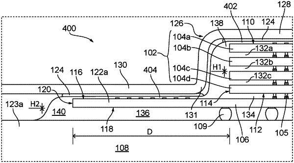
1. A semiconductor die assembly, comprising:
a first semiconductor die having an upper surface, an edge surface extending from a perimeter portion of the upper surface, and a first footprint;
a second semiconductor die carrying the first semiconductor die, wherein the second semiconductor die has a second footprint larger than the first footprint such that the second semiconductor die includes a peripheral portion extending beyond the first footprint;
a heat spreader thermally coupled to the first semiconductor die and to the peripheral portion of the second semiconductor die;
a molded underfill material extending at least partially over the upper surface of the first semiconductor die, along the edge surface of the first semiconductor die, and over the peripheral portion of the second semiconductor die;
a first planar thermal interface feature having a first side in direct contact with a first portion of the molded underfill material disposed over the upper surface of the first semiconductor die and an opposite second side in direct contact with the heat spreader; and
a second planar thermal interface feature having a first side in direct contact with a second portion of the molded underfill material disposed over the peripheral portion of the second semiconductor die, and an opposite second side in direct contact with the heat spreader.
|