| CPC H01L 25/18 (2013.01) [H01L 23/481 (2013.01); H01L 23/5386 (2013.01); H01L 24/13 (2013.01); H01L 24/81 (2013.01); H01L 25/0652 (2013.01); H01L 2924/1431 (2013.01); H01L 2924/1436 (2013.01)] | 20 Claims |
|
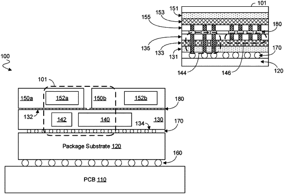
1. A system comprising
a first integrated circuit (IC) die including first integrated circuitry;
a second IC die including:
first contacts disposed in or on a first side of the second IC die, wherein the second IC die is coupled to the first IC die via the first contacts;
second contacts disposed in or on a second side of the second IC die, the second side opposite the first side;
second integrated circuitry including first active circuit elements to communicate with the first integrated circuitry;
first interconnects each extending to the first side and to the second side; and
second interconnects each coupled between the first side and the second integrated circuitry, wherein the first interconnects and the second interconnects each to couple to the first IC die via a respective one of the first contacts; and
a display device coupled to the first IC die via the second IC die, the display device to display an image based on a signal output by the second IC die.
|