| CPC H01L 25/18 (2013.01) [H01L 23/481 (2013.01); H01L 23/5226 (2013.01); H01L 23/544 (2013.01); H01L 24/08 (2013.01); H01L 2223/54426 (2013.01); H01L 2224/0224 (2013.01); H01L 2224/08145 (2013.01)] | 20 Claims |
|
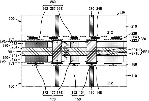
8. A semiconductor package comprising a first semiconductor chip, a second semiconductor chip, and at least one first bonded pad connecting the first and second semiconductor chips,
wherein the first semiconductor chip comprises:
a first semiconductor substrate comprising a first semiconductor element on a first active surface thereof;
a plurality of first front surface pads disposed on the first active surface of the first semiconductor substrate;
at least one first penetrating electrode penetrating at least a portion of the first semiconductor substrate and connected to the first front surface pads;
a first rear surface cover layer disposed on a first inactive surface of the first semiconductor substrate; and
a first rear surface dummy conductive layer comprising a first rear surface alignment pattern and penetrating a portion of the first rear surface cover layer;
wherein the second semiconductor chip comprises:
a second semiconductor substrate stacked on the first semiconductor chip, and comprising a second semiconductor element on a second active surface thereof;
a second front surface cover layer disposed on the second active surface; and
a second front surface dummy conductive layer comprising a second front surface alignment pattern separated apart from the first rear surface alignment pattern and penetrating a portion of the second front surface cover layer; and
wherein the first bonded pad penetrates the first rear surface cover layer and the second front surface cover layer, and is connected to the first penetrating electrode.
|