| CPC H01L 25/167 (2013.01) [G06V 10/147 (2022.01); G06V 40/1318 (2022.01); H01L 25/18 (2013.01)] | 9 Claims |
|
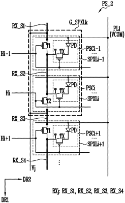
1. An input sensing device, comprising:
a power line;
driving lines;
a first signal line including a first sub-line, a second sub-line, and a third sub-line;
a second signal line connected to the first signal line; and
sensor pixel groups connected to the power line, the driving lines, and the first signal line,
wherein at least one sensor pixel group among the sensor pixel groups includes:
a first optical sensor for transferring a photoelectrically converted charge from the power line to the second sub-line in response to a driving signal provided through a first driving line among the driving lines;
a second optical sensor for transferring a photoelectrically converted charge from the power line to the second sub-line in response to a driving signal provided through a second driving line among the driving lines; and
a first transistor connected between the first sub-line and the second sub-line, wherein the first transistor includes a gate electrode connected to the first driving line.
|