| CPC H01L 25/167 (2013.01) [H01L 24/92 (2013.01); H01L 27/124 (2013.01); H01L 27/1259 (2013.01); H01L 33/60 (2013.01); H01L 33/62 (2013.01); H01L 2224/9201 (2013.01); H01L 2224/92144 (2013.01); H01L 2933/0066 (2013.01)] | 6 Claims |
|
1. A method of fabricating a display device, the method comprising:
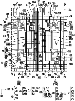
preparing a substrate comprising a display area having a pixel area in which each pixel is located and a non-display area;
forming, on the substrate, a first conductive layer comprising a plurality of fan-out lines and a plurality of scan lines;
forming an interlayer insulating layer on the first conductive layer;
forming, on the interlayer insulating layer, a second conductive layer comprising a plurality of data lines, a plurality of first bridge lines respectively connected to corresponding fan-out lines from among the fan-out lines, and a plurality of second bridge lines respectively connected to corresponding fan-out lines from among the fan-out lines;
forming, over the second conductive layer, a passivation layer including a plurality of contact holes exposing a portion of each of the plurality of first bridge lines, a portion of each of the plurality of second bridge lines, and a portion of each of the plurality of data lines;
forming a first alignment electrode on the passivation layer, the first alignment electrode electrically connected to the plurality of first bridge lines, a second alignment electrode electrically connected to the plurality of second bridge lines, and a third alignment electrode electrically connected to the plurality of data lines;
supplying light emitting elements in the pixel area, forming an electric field between the first to third alignment electrodes by applying a corresponding alignment voltage to each of the plurality of first bridge lines, each of the plurality of second bridge lines, and each of the plurality of data lines, and aligning the light emitting elements between the first to third alignment electrodes; and
forming a first electrode and a first sub-electrode that are spaced from each other, by removing a portion of the first alignment electrode, and forming a third electrode and a second sub-electrode that are spaced from each other, by removing a portion of the third alignment electrode.
|