| CPC H01L 25/16 (2013.01) [H01L 24/19 (2013.01); H01L 24/20 (2013.01); H01L 24/24 (2013.01); H01L 24/73 (2013.01); H01L 2224/2201 (2013.01); H01L 2224/221 (2013.01); H01L 2224/244 (2013.01); H01L 2224/24145 (2013.01); H01L 2224/24265 (2013.01); H01L 2224/73204 (2013.01); H01L 2224/73209 (2013.01); H01L 2224/73217 (2013.01); H01L 2224/73259 (2013.01)] | 10 Claims |
|
1. A method of fabricating a fan-out chip package, the method comprising following steps:
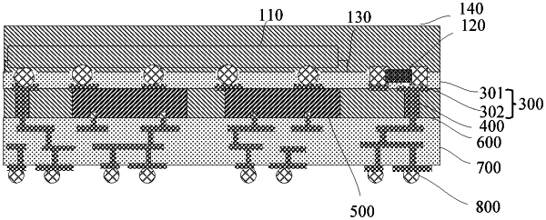
providing a support substrate, and forming a separation layer on the support substrate;
forming a first redistribution layer on the separation layer, wherein the first redistribution layer comprises a first surface in contact with the separation layer and a second surface opposite to the first surface;
forming metal connecting posts on the second surface of the first redistribution layer, wherein the metal connecting posts are electrically connected to the first redistribution layer;
providing a semiconductor chip, wherein the semiconductor chip is disposed on the second surface of the first redistribution layer, wherein a back side of the semiconductor chip is bonded to the first redistribution layer, and a front side of the semiconductor chip is facing away from the second surface of the first redistribution layer;
packaging the first redistribution layer, the metal connecting posts, and the semiconductor chip by a first packaging layer, wherein the metal connecting posts and a pad of the semiconductor chip are configured to be exposed from the first packaging layer;
forming a second redistribution layer on the first packaging layer, wherein the second redistribution layer comprises a first surface in contact with the first packaging layer and a second surface opposite to the first surface, and the second redistribution layer is electrically connected to the metal connecting posts and the pad of the semiconductor chip;
forming metal bumps on the second surface of the second redistribution layer, wherein the metal bumps are electrically connected to the second redistribution layer;
providing a carrier, and peeling off the support substrate to expose the first surface of the first redistribution layer;
performing laser etching on the first redistribution layer to expose a metal distribution layer in the first redistribution layer;
providing a stacked chip package and a passive element, wherein the stacked chip package and the passive element are located on the first surface of the first redistribution layer, wherein the stacked chip package is electrically connected to the metal distribution layer via contact bumps exposed from the first redistribution layer, and wherein the passive element is electrically connected to the metal distribution layer via a contact pad exposed from the first redistribution layer;
filling a gap between the stacked chip package and the first redistribution layer with a filling layer;
packaging the first redistribution layer, the stacked chip package, and the passive element by a second packaging layer;
and
performing cutting to form the fan-out chip package structure.
|