| CPC H01L 25/0657 (2013.01) [H01L 23/5226 (2013.01); H01L 23/5389 (2013.01); H01L 24/08 (2013.01); H01L 24/09 (2013.01); H01L 25/50 (2013.01); H01L 2224/08146 (2013.01); H01L 2224/0912 (2013.01)] | 20 Claims |
|
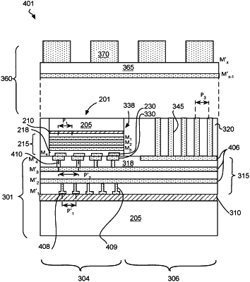
1. An integrated circuit (IC) device structure, comprising:
a first IC chip comprising a first device layer and a first metallization layer interconnected to transistors of the first device layer;
a second IC chip over a first region of the first IC chip, the second IC chip comprising a second device layer and a second metallization layer interconnected to transistors of the second device layer; and
a third metallization layer over a second region of the first IC chip, and adjacent to an edge of the second IC chip, the third metallization layer interconnected to transistors of at least one of the first or second device layers.
|