| CPC H01L 25/0657 (2013.01) [H01L 21/4853 (2013.01); H01L 21/4857 (2013.01); H01L 21/565 (2013.01); H01L 23/3121 (2013.01); H01L 23/49822 (2013.01); H01L 23/552 (2013.01); H01L 24/48 (2013.01); H01L 2224/48227 (2013.01); H01L 2225/0651 (2013.01); H01L 2225/06506 (2013.01); H01L 2225/06537 (2013.01); H01L 2225/06562 (2013.01); H01L 2225/06582 (2013.01); H01L 2924/3025 (2013.01)] | 9 Claims |
|
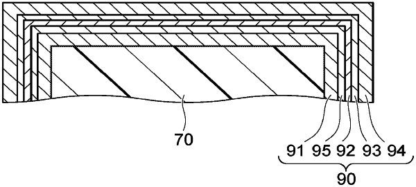
1. A semiconductor package comprising:
a substrate;
a semiconductor chip provided on the substrate;
a resin layer configured to cover the semiconductor chip on the substrate; and
a metal film configured to cover a surface and side surfaces of the resin layer, wherein
the metal film is a laminated film including
a first metal layer configured to cover the resin layer,
a second metal layer including a first metal material that is different from a material of the first metal layer,
a third metal layer including an alloy of the first metal material forming the second metal layer and a second metal material different from the first metal material, the second metal material included in the third metal layer being 1 to 20 atomic percent (at. %), and
a fourth metal layer configured to cover the second or third metal layer, wherein
a grain size in the second metal layer is 0.10 μm or more,
a grain size in the third metal layer is less than 0.10 μm,
a total thickness of the second and third metal layers is in a range of 0.45 μm to 2.5 μm,
a resistance value of the second metal layer is lower than resistance values of the first, third, and fourth metal layers,
the second metal layer is provided on the first metal layer,
the third metal layer is provided on the second metal layer, and
the fourth metal layer is provided on the third metal layer.
|