| CPC H01L 25/0655 (2013.01) [H01L 21/56 (2013.01); H01L 23/14 (2013.01); H01L 23/31 (2013.01); H01L 23/49811 (2013.01); H01L 23/5386 (2013.01); H01L 23/544 (2013.01); H01L 24/14 (2013.01)] | 20 Claims |
|
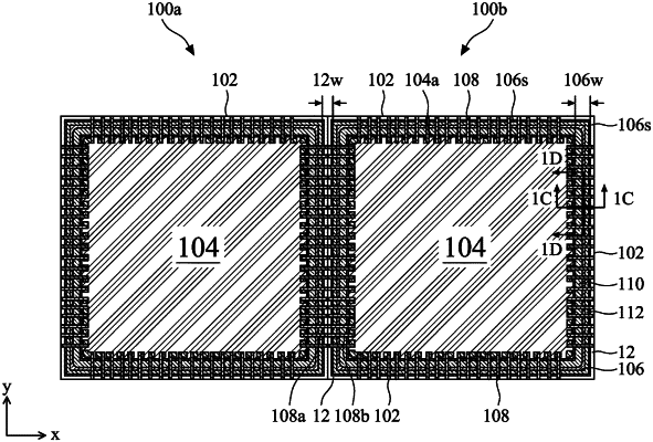
1. A method for forming a semiconductor device, comprising:
forming a first integrated circuit die having a first edge interconnect feature, and a second integrated circuit die having a second edge interconnect feature, wherein the first integrated circuit die is diced along a first cutting surface and the second integrated circuit die is diced along a second cutting surface, the first edge interconnect feature is exposed on the first cutting surface of the first integrated circuit die, and the second edge interconnect feature is exposed on the second cutting surface of the second integrated circuit die;
positioning the first and second integrated circuit dies adjacent to each other such that the first edge interconnect feature faces the second edge interconnect feature; and
forming an inter-chip connector between the first edge interconnect feature and the second edge interconnect feature.
|