| CPC H01L 25/0652 (2013.01) [H01L 23/49822 (2013.01); H01L 25/50 (2013.01)] | 20 Claims |
|
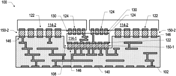
1. A microelectronic assembly, comprising:
a package substrate;
a plurality of first dies; and
a plurality of second dies, wherein at least one of the second dies is coupled to at least two of the first dies with first interconnects, and at least one of the second dies is coupled to the package substrate with second interconnects, wherein the first interconnects include:
a first set of conductive contacts on the at least one of the second dies that is coupled to the at least two of the first dies, the first set of conductive contacts bonded with conductive contacts on a first one of the least two of the first dies, and a second set of conductive contacts on the at least one of the second dies that is coupled to the at least two of the first dies, the second set of conductive contacts bonded with conductive contacts on a second one of the least two of the first dies.
|