| CPC H01L 24/82 (2013.01) [H01L 24/25 (2013.01); H01L 2224/04105 (2013.01); H01L 2224/06181 (2013.01); H01L 2224/2518 (2013.01); H01L 2224/8284 (2013.01); H01L 2224/82104 (2013.01); H01L 2924/13091 (2013.01)] | 5 Claims |
|
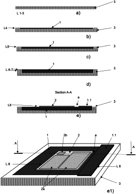
1. A method for contacting and packaging a semiconductor chip of a power electronic component, wherein the power electronic component has a first, lower contact face and a semiconductor chip positioned thereon, characterized in that a ceramic insulation layer, which surrounds the semiconductor chip along its circumference and extends over the first, lower contact face not covered by the semiconductor chip, is printed onto the first, lower contact face, and in that a second, upper contact face of the power electronic component is printed onto the ceramic insulation layer and the semiconductor chip, wherein the first, lower and second, upper contact face and the ceramic insulation layer are created in a printing process by means of a 3D multi-material printer such that,
in a first method step, the first, lower contact face made of an electrically conductive material is produced by means of the multi-material printing process,
in a second method step, the semiconductor chip is placed, oriented and positioned onto the first, lower contact face,
in a third method step, a ceramic insulation layer, which surrounds the circumference of the semiconductor chip, is printed onto the first, lower contact face via the 3D multi-material printing process, a height of said ceramic insulation layer substantially corresponding to a height of the semiconductor chip, as a result of which a flat surface consisting of the upper side of the semiconductor chip and the ceramic insulation layer is formed as a support for the second, upper contact face,
in a fourth method step, the second, upper contact face made of an electrically conductive material is printed onto the ceramic insulation layer and the semiconductor chip via the 3D multi-material printing process,
in a fifth method step, a housing for the semiconductor chip is created by means of the printing process,
in a sixth method step, the power electronic component is sintered by means of heat treatment.
|