| CPC H01L 24/81 (2013.01) [B23K 26/50 (2015.10); H01L 24/75 (2013.01); B23K 2101/40 (2018.08); H01L 2224/75263 (2013.01); H01L 2224/81048 (2013.01); H01L 2224/81201 (2013.01); H05K 2201/068 (2013.01)] | 21 Claims |
|
1. A method to manufacture a semiconductor device, comprising:
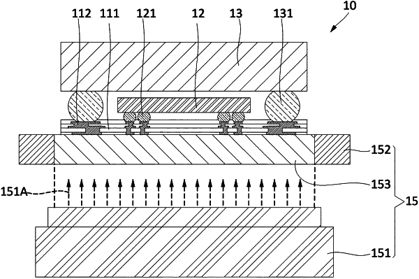
providing an electronic component over a substrate, the electronic component comprising a body comprising silicon and an interconnect comprising a metal, wherein the interconnect of the electronic component contacts a conductive structure of the substrate;
providing the substrate over a laser assisted bonding (LAB) tool, wherein the LAB tool comprises a stage block comprising a window, wherein the window of the stage block comprises a solid translucent material; and
heating the interconnect with a laser beam through the window until the interconnect is bonded with the conductive structure;
wherein more heat is applied to the interconnect than to the body of the electronic component;
wherein the stage block supports the window and the substrate over the laser beam, and wherein the laser beam is directed at the interconnect through a bottom side of the window and through the substrate without passing through the electronic component;
wherein the substrate is on the window, and the window is configured to support the substrate; and
wherein a footprint of the window is as large or larger than a footprint of the substrate.
|